|

|
|

| Ask the Experts | |||||||
|
|||||||
|
March 20, 2024 - Updated January 26, 2015 - Originally Posted QFN Open Solder Joints
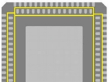
See the yellow area in the photo. Usually only 1 or 2 pads have opens. Our boards are double side reflow and this component is mounted on the first side. What is happening? M.N. |
|||||||
| Expert Panel Responses | |||||||
|
There are lots of variable when installing these types of components of which some are definitely more important than others. If they are happening as stated only on the inner row of pads I would check the reflow profile to verify the reflow temperature is met at these locations. I would also recommend checking for the thermal differences in the associated pads or land areas. Anything connected to an inner layer will require longer dwell time to verify the connection is made. Check the amount of solder paste applied to the ground plane area to verify the molten solder does not raise the component creating opens with the solder joint on the second row. From a stencil perspective check the aperture openings to make sure they are correct and the correct amount of paste is deposited on those pads. In certain cases where we've seen this situation larger paste deposition was required. From a board perspective check to see if there are any vias in the areas of the pads as this will draw the solder away from the pads and create an insufficient solder condition on the pad.
Vice President, Technical Director EPTAC Corporation At EPTAC Corporation, Mr. Lambert oversees content of course offerings, IPC Certification programs and provides customers with expert consultation in electronics manufacturing, including RoHS/WEEE and lead free issues. Leo is also the IPC General Chairman for the Assembly/Joining Process Committee.
I would validate the amount of paste being deposited in the center/thermal area.If there it is 1:1 aperture to pad, then you are most likely "floating" your part just enough to cause the problem. To alleviate this issue, do a windowpane on the stencil aperture to reduce the solder paste deposition around 10-15%.
Manufacturing Engineer Esterline Interface Technologies Mr. Hughes has been in the electronics manufacturing field for 20 years. Operating the processes and as a manufacturing engineer for the last 14 years. He is also a CIT as well as an SMTA Certified Process Engineer.
I'd recommend you review your land pattern design, reflow settings, solder mask,amount of solder paste being deposited on those pads. Pay special attention to the thermal plane and, if possible minimize the amount of solder deposited on the thermal plane.
Senior Manufacturing Engineer Northrop Grumman Edithel is a chemical engineer with 20 year experience in manufacturing & process development for electronic contract manufacturers in US as well as some major OEM's. Involved in SMT, Reflow, Wave and other assembly operations entailing conformal coating and robotics.
My suspicion is that possibly during the initial reflow, but more likely during the second reflow, row 1 (the outside row) is robbing row 2 (the inside row) of solder, causing an open. It does not have to take very much solder from the inside row for this to happen, and it may not be readily apparent in an X-ray,because the solder balls on the outside row may not be appreciably larger when this happens. I also suspect that it is happening mostly because you are printing solder paste with an aperture reduction that is only perhaps 5%-10%smaller than the pads on the PWB and any imperfection in the paste print, even a few tiny solder fines between the pads of row 1 and row 2 at the diagonal corners would be enough to cause this solder thieving to happen, especially during the 2nd reflow. During the second reflow, you not only have the large blob of solder on the belly pad causing the part to float around upside down, but any conveyor vibration or motion that causes movement of the part can set off the thieving. A component of this size is going to warp or cupat least a small amount. If any cupping occurs during the second reflow the pressure in the z-axis is more pronounced on the inner row than the outer row,so the solder will wick outward, from the inner to the outer row. I recommend you simply try applying a good corner bonding adhesive to the outside corners of the component after reflow, wash, touch-up and rework is completed for side one. A good snap-cure corner bonding adhesive such as Loctite 4621 or any number of others can be used. I would even go so far as to recommend a water soluble temporary maskant be tried as a corner bond adhesive, that has worked well for me but you need to be careful, not all soluble masks are created equal. As the CCA goes into the reflow oven for side two, the corner bond material cures prior to reflow temperatures, so even if the component's solder joints do go into liquidus the corner bonds will prevent any component movement. Later you can either wash away the temporary maskant as part of the second-side machine cleaning, or you can simply leave the corner bonding adhesive on which would require an ECN with approval from the customer (but it does improve long term reliability). As a minimum, I would simply try this on a small batch of CCAs to see if the corner bonding (whether temporary or permanent) AND controlling the paste registration, print setup, etc., fix the issue. If no opens appear on the tryout batch, further qualify the process to ensure no other harmful effects are introduced. Qualify, qualify, qualify. The wall between engineering and production is never high enough, and sometimes the temptation to throw process changes over the wall before full qualification is too tempting.
Advanced Engineer/Scientist General Dynamics Richard D. Stadem is an advanced engineer/scientist for General Dynamics and is also a consulting engineer for other companies. He has 38 years of engineering experience having worked for Honeywell, ADC, Pemstar (now Benchmark), Analog Technologies, and General Dynamics.
If you are experiencing opens with a QFN or in this case DR QFN, reflow is not occurring evenly or something is holding the part up. I would review the datasheet for this component and make sure the pad design matches your pcb. Also make sure the stencil design and paste type matches your process. The thermal pad should have a window frame cut outwith different size And dimensions based on the lead pitch. Also make sure you have a robust profile allowing enough time for wetting to occur. For this package, a post print inspection is very important. Without knowing your board layout or part size, I can only suggest this type of part is typically placed and reflowed at second pass. If this is not possible, you may want to check for opens after the first Reflow to see if its opening there or at the second reflow.
Manufacturing Applications Specialist Cirtronics Corp. Mr. Bush has over 30 years of experience in electronics contract manufacturing. Major areas of expertise include through-hole, SMT, wave, and selective soldering.
There are two possible causes: It could be that the open is the result of insufficient solder paste. Make sure that your solder paste is capable of adequate transfer efficiency for that aperture size. If there is a trend in the location of the open(s), it could be the result of a bad aperture(s) in the stencil. It is also possible that there may be too much paste on the center pad. During reflow the package can become buoyant on the solder on the center pad. This can actually lift the package up and cause it to lose contact with the peripheral pad(s) creating an open.
Technical Support Engineer Indium Corporation Kay Parker is a Technical Support Engineer based at Indium Corporation's headquarters in Clinton, N.Y. In this role she provides guidance and recommendations to customers related to process steps, equipment, techniques, and materials. She is also responsible for servicing the company's existing accounts and retaining new business.
With limited data, I can only guess at this time.
Engineering and Operations Management Independent Consultant Georgian Simion is an independent consultant with 20+ years in electronics manufacturing engineering and operations.
Contact me at georgiansimion@yahoo.com. Reader Comment
For us, it was all about the printing. Good aspect ratios and Nano coating solved the problem.
Joe laganella, Swemco
|
|||||||
| Submit A Comment | |||||||
|
Comments are reviewed prior to posting. You must include your full name to have your comments posted. We will not post your email address. |


|
Free Newsletter Subscription
Circuitnet is built for professionals who bear the responsibility of looking ahead, imagining the future, and preparing for it. Insert Your Email Address |
|


|