|
|
|
|
|
|
|
|
|
|
|
|
| Ask the Experts | |||||||
|
|||||||
|
March 19, 2024 - Updated December 10, 2014 - Originally Posted BGA BAll Sheer Testing
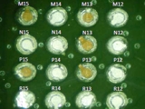
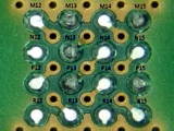
In some areas the pad was ripped off the circuit board surface and remained attached to the BGA ball. In other areas the joint sheered at the ball/pad interface. What should we expect to see? Should all the joints act the same way? Is one attachment result better than the other? T.S.Y. |
|||||||
| Expert Panel Responses | |||||||
|
When a BGA is sheered from its terminations, the separation is going to take place at the weakest points. Some may separate at the solder ball, some at the pad to board connection. It depends on the strength of the pad, solder mask, solder ball density, as well as a good solder joint. If the joint sheered at the ball/pad connection, that would indicate a poor solder connection. Typically you Would expect to lose the ball from the BGA, or the pad from the PCB.
Manufacturing Applications Specialist Cirtronics Corp. Mr. Bush has 20 years experience in electronics contract manufacturing. Major areas of expertise include through hole, SMT, wave and selective soldering.
That is exactly the results I would expect from a mechanical removal of a BGA. Remember solder is designed to join two metals for an electrical connection, it is not like a weld and meant to resist the forces you applied by removal. What was the reason behind this? Have you been seeing failures with this device or just an assumption that there were solder issues? Do you X-ray? For BGA process troubleshooting I recommend doing a dye and pry over just a removal. The dye will penetrate voids and can help isolate bad solder connections. You will see the dye either on the part or on the board after it was pried.
Process Engineer Esterline Interface Technologies Mr. Pierowski is currently a Process Engineer for SMT and Electrical Assembly with 20+ years of experience. A majority of the experience was based in screen/stencil printing for electronics manufacturing including application support for SMT, LTCC, HTCC and thick film.
I have pulled and sheered many BGAs from assemblies to access flux removal under devices. I commonly see both pad and solder failure on the same site. Not all solder connections are the same even under the same device. Solder print volumes are not the same and not all pads reflow at the same moment in time giving rise to metallurgical and solder voiding differences. Having said all of that, in a controlled tensile pull, one should expect a well designed BGA connection to fail by pulling the pad rather than the solder connection failing.
President Austin American Technology Founder and President of AAT. Steve holds numerous patents and has authored numerous research papers and articles in cleaning and soldering. Steve is a founding member of the Central Texas Electronics Association and is a past Director of IMAPS. Steve is active on several IPC cleaning committees.
The goal of a shear test is to see the BGA "break" which points toward a ductile fracture. What you are seeing in your tests when the pad is ripped off is that the bond between BGA and pad is stronger that the bond between BGA and substrate. In other areas where the joint sheared is a sign of a brittle joint. This is just a tiny bit of information without knowing the surface finish of the PCB, the equipment used for the pull and its settings. My recommendation would be to research about similar experiments conducted using JESD22-B117A and try to see if you can duplicate the results.
Senior Manufacturing Engineer Northrop Grumman Edithel is a chemical engineer with 20 year experience in manufacturing & process development for electronic contract manufacturers in US as well as some major OEM's. Involved in SMT, Reflow, Wave and other assembly operations entailing conformal coating and robotics.
I would expect the separation to happen at the board level (solder joint to the pad) and/or at the component level (solder ball to the component body). One is not better or worse than the other one. There are some variances in the process that can help towards one of the results or the other (solder paste deposition volume, oxidation level, positioning on the component area - inside, outside, etc.). If the solder connection itself is not breaking apart, it means that the soldering process is effective. Is that what the experiment was about?
Engineering and Operations Management Independent Consultant Georgian Simion is an independent consultant with 20+ years in electronics manufacturing engineering and operations.
Contact me at georgiansimion@yahoo.com. What you are seeing is what is expected. However keep in mind. If your objective was to purely test the shear test the BGA for mechanical strength, then you should not be worried about the what the soldering would look like. If you are doing to tests to confirm mechanical strength and solder joints then conduct a dye and pry with the test. The dye-n-pry method allows for the failed solder joint to be marked with a dye regardless of the location in the BGA. Additionally, one can visually inspect the package after the pry operation to identify the failed solder joint and determine the cause for the failure.After completing the dye application, once the dye has cured, the BGA is ready to be removed from the PCB. The goal in removing the BGA is to fully break all of the good solder joints that exist between the BGA and PCB, thereby exposing the open joint that will be evident by the colored dye that has filled the crack or gap of the open connection. The good solder connections that were broken after dye curing will show either silver/gray solder or copper solder pads torn completely out of the BGA and PCB. Understanding the root cause of the various types of failed solder interconnects requires high level of experience at solder joint analysis, for this specific analysis we only looking at cold joints or no joints. Also ensure that before both testing,X-Ray your PCB, to check alignment and voiding.
Process Engineering Manager - Electronics Altech UEC, South Africa Currently with Altech UEC and responsible for technology road map in PCBA electronic manufacturing and technical support for PCBA electronic manufacturing for Altech UEC and its JDM's. Over 7 years in SMT, Radial Insertion, Wave solder & Test Applications.
Reader Comment
Ideally all BGA balls should behave alike. But in practical it need not. It depends on the position of the ball, the stiffness of the built-in PCB of the BGA device etc. Each BGA device shall withstand a specified shear force based on the total number solder balls attached. If it is withstanding the force based on MIL-HDBK-883K Method 2019.9, one can say the overall soldering is good. However, prior to subjecting the device to shear tests, one has to ensure with X-ray imaging, that voids in the solder joints are 30% or less for Class 1,2, 3 as per IPC 610G. During shear testing process, if the balls gets detached from the BGA (Built-in-PCB) device or from the external PCB or pad getting ripped off the circuit along with the solder balls and solder balls per se are fine, one cannot consider that the shear test is complete. One can conclude that the solder strength is higher than the peel strength of the PCB.
Dr. KUTTIYIL THOMAS OOMMEN THARAKAN, VSSC
|
|||||||
| Submit A Comment | |||||||
|
Comments are reviewed prior to posting. You must include your full name to have your comments posted. We will not post your email address. |


|
Free Newsletter Subscription
Circuitnet is built for professionals who bear the responsibility of looking ahead, imagining the future, and preparing for it. Insert Your Email Address |
|
|
|
|
|
|
|
|