|
|
|
|
|
|
|
|
|
|
|
|
| Ask the Experts | |||||||
|
|||||||
|
January 26, 2022 - Updated December 11, 2013 - Originally Posted Automatic Insertion Causing Plated Hole Damage
We need to use a mechanical clinching method per the customer request. These 2 pin components must sit flat on the PCB, with no tilt. What can we do to reduce or eliminate the plated hole damage. What is the criteria for acceptability of cracks and deformation of the plated hole wall? M.C. |
|||||||
| Expert Panel Responses | |||||||
|
Interesting question. Sometimes I believe the customer has to be educated and this may be the case in this situation. The condition caused by the clinching of the leads is damaging the product and will cause catastrophic failures in the product. All the IPC specifications mention in the clinching section that large pins or tempered leads are not to be clinched due to this potential plated through hole damage occurring from the clinching operation. If the connector needs to be flat to the board, perhaps an alternative method should be used to secure the component to the laminate material, such as an adhesive. Alternative methods such as manually soldering the component in place would produce a more reliable connection than continuing trying to meet the requirements of the customer as defined by their documentation. IPC-A-610 Rev E, page 7-38 explicitly states that tempered leads shall not be terminated with a full clinch configuration, and even partial clinch with such large leads will cause damage to the plated through hole barrel. IPC-A-600 Rev H, page 99, section 3.3.6 discusses plating cracks and they are not allow for any class of products. This is a design issue that must be addressed by the user and supplier as this condition is not acceptable under any circumstance.
Vice President, Technical Director EPTAC Corporation At EPTAC Corporation, Mr. Lambert oversees content of course offerings, IPC Certification programs and provides customers with expert consultation in electronics manufacturing, including RoHS/WEEE and lead free issues. Leo is also the IPC General Chairman for the Assembly/Joining Process Committee.
Intrusive reflow could solve the problem. Board would need to be redesigned for non-press fit holes.
Vice President Technology Photo Stencil For over 18 years, Dr. Coleman has been the vice president of technology for Photo Stencil, working closely with customers to understand their printing requirements. His efforts have resulted in several new stencil products.
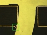
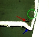
PTH is likely to get damaged if the part lead is stiff and not clinchable easily.Hence it is necessary to check if the lead diameter and / or material of the lead suitable for clinching. Second a proper clinching tool is to be used that gives acceptable clinch. It is also necessary to check the thickness of the copper and solder plating at the corner of the PCB and it should be greater than 1 micron minimum. From the picture it is evident that the component is sitting flat on the PCB and the constraint point on the Component side of the lead is not available to provide acceptable clinch. This is a clear non-clinchable type of mounting.
Head-Quality Astra Microwave Products, Hyderabad, AP India Holds Degree in Engineering, started off as Scientist/Engineer in ISRO (Indian Space Research Organization) in Quality Assurance of Space hardware Electronics Production. Worked in the area of Parts, Material and Process; DPA, FA and Process Qualification for space and ground hardware. Later moved into Private sector and worked in the area of Quality Management Systems & ISO 9001 certification. Currently hold a position as Head-Quality in RF/Microwave Product manufacturing for Defense and Aerospace segment.
After seeing the images, it is pretty obvious that this design is not suitable for clinching. There are selective soldering methods including hand placing (if feasible) that will ensure that a correct/conforming solder joint is achieved and the clinch operation is not necessary. Design change is costly but a slight change in the process requirements can fix the problem. Recommendations can be made to fix this issues and the final decision will be in your customer's court.
Engineering and Operations Management Independent Consultant Georgian Simion is an independent consultant with 20+ years in electronics manufacturing engineering and operations.
Contact me at georgiansimion@yahoo.com. |
|||||||
| Submit A Comment | |||||||
|
Comments are reviewed prior to posting. You must include your full name to have your comments posted. We will not post your email address. |


|
Free Newsletter Subscription
Circuitnet is built for professionals who bear the responsibility of looking ahead, imagining the future, and preparing for it. Insert Your Email Address |
|
|
|
|
|
|
|
|