|
|
|
|
|
|
|
|
|
|
|
|
| Ask the Experts | |||||||||||
|
|||||||||||
|
November 19, 2021 - Updated July 30, 2013 - Originally Posted BGA Joint Voids - Accept or Reject?
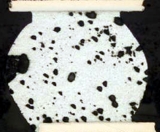
I have heard that some level of voids within a BGA solder joint can actually improve reliability. Is this true? E.W. |
|||||||||||
| Expert Panel Responses | |||||||||||
|
Too many voids at the interface. Single voids in the bulk of the solder play little role in time to failure. Interfacial voiding can cause significant reductions.
CEO & Managing Partner DfR Solutions Dr. Hillman's specialties include best practices in Design for Reliability, strategies for transitioning to Pb-free, supplier qualification, passive component technology and printed board failure mechanisms.
Reject the joint, the level of voids and where they are would look to be too high, I would x-ray a component that has not been reflowed to see if the balls are already failed.
Global Product Champion Henkel Electronics Richard Boyle is a Global Product Champion at Henkel Electronics. He has over 25 years experience in the electronics assembly industry and is responsible for the global technical service of all of Henkel's solder materials.
This looks like excessive voiding. However, without a tool (like X-Ray voiding % check) that will give you a quantitative result, this is just an impression. Definitely something that you want to minimize. I do not know about increased reliability but this is obvious sign that the outgassing of the solder in the reflow process is not completed - there is a lot still trapped in the material. It is not uncommon to see voiding especially with lead-free solder that has more outgassing. Check your oven profile - usually a longer soak and a lower reflow temperature provides better results from the voids elimination point of view.
Engineering and Operations Management Independent Consultant Georgian Simion is an independent consultant with 20+ years in electronics manufacturing engineering and operations.
Contact me at georgiansimion@yahoo.com. Let's first address the question of IPC-610 acceptability. The acceptability criterion for voiding in IPC-610 is currently <25% void area on transmission x-ray. This image is a cross section, which is not directly comparable to an x-ray, because only the voids at the plane of section are visible. When viewing a transmission x-ray image, all voids, regardless of where they lie in the joint, are visible. This image contains 16.7% void area at the plane of section, as determined using a "threshold" image transformation in Adobe Photoshop. That's high. Based on this, I'd expect an x-ray image of the joint to show at least 25% voiding. If (and I emphasize if) that is so, the joint would be a reject per IPC-610 or J-STD-001. Now, let's look at the practical side. The voids in this joint are not localized at the component or PWB interface, but are evenly distributed throughout the joint. Current research seems to indicate that in this situation, the voiding is unlikely to have a negative effect on reliability. It is, however, a process indicator. Were this joint a product of my manufacturing process, I would be investigating the root cause(s) and optimizing the process to reduce the occurrence of the voids. For some additional reading on the matter, look at this article published by IPC, and consider reading the referenced paper.
Process Engineer Astronautics Fritz's career in electronics manufacturing has included diverse engineering roles including PWB fabrication, thick film print & fire, SMT and wave/selective solder process engineering, and electronics materials development and marketing. Fritz's educational background is in mechanical engineering with an emphasis on materials science. Design of Experiments (DoE) techniques have been an area of independent study. Fritz has published over a dozen papers at various industry conferences.
If this was mine I would reject as it doesn't appear to have reflowed correctly nor does it appear to have paste printed on the pad at all. So my guess looking at the picture is
Lastly use T4 powder for dense prints = less voids.
Technical Sales Manager BLT Circuit Services Ltd Greg York has over thirty two years of service in Electronics industry. York has installed over 600 Lead Free Lines in Europe with Solder and flux systems as well as Technical Support on SMT lines and trouble shooting.
Here's my thoughts:
Design Engineering Lockheed Martin Space Systems Mike Green is co-chairman of the IPC Terms and Definitions Committee. He has been working with board design and manufacturing for 33 years.
Of all the voids I've looked at, none have shown this type of characteristics. I would ask how this solder ball was made and conduct an evaluation of the solderability of the material to verify the goodness of the paste and the flux. Secondly, since this does not look like anything we've ever looked at, it would create some questions in my mind as to its goodness and reliability. Therefore since this is unknown, I would reject this condition, from the perspective that you don't have a homogeneous solder joints, and the joint interface is loaded with planar voids.
Vice President, Technical Director EPTAC Corporation At EPTAC Corporation, Mr. Lambert oversees content of course offerings, IPC Certification programs and provides customers with expert consultation in electronics manufacturing, including RoHS/WEEE and lead free issues. Leo is also the IPC General Chairman for the Assembly/Joining Process Committee.
This is a difficult call on a generalization of voids, but I would remind you this is a thin section of the bigger ball and the amount of voids that can be seen on the ball to pad interface would concern me and suggest that the boards with these voids be temperature cycled to assess the joint integrity and determine if this amount of voiding has a negative or positive affect on the balls.
President/Senior Technical Consultant Foresite Mr. Munson, President and Founder of Foresite, has extensive electronics industry experience applying Ion Chromatography analytical techniques to a wide spectrum of manufacturing applications.
What you have heard about voids increasing mechanical reliability in BGA solder joints is not necessarily untrue. I am familiar with research conducted by Glen Dody of Motorola in the 90's that found voids in the bulk solder would tend to terminate cracks that were propagating. In the section you have shown I would be concerned about the amount of voiding at the inter-metallic compound (IMC) interface. While voids in the bulk solder might stop a crack, the IMC is the weakest mechanical location in the solder joint. Voids along this interface will tend to promote propagation as a separation occurs at the IMC. I would work to reduce voiding in your process.
President Process Sciences, Inc. Stephen Schoppe is President of Process Sciences, Inc., and has 19 years experience providing SMT services to electronics manufacturers. Stephen provides consulting to several Fortune 500 clients on solder and SMT processes, and is a frequent guest speaker at SMT industry events.
This BGA definitely has too much voiding and needs to be corrected. Whenever this much voiding forms in a single BGA, it is an indication of a poor solder joint formation. This could be due to either weak flux activity or excessive solder powder oxidation. Mixing two different solder powders also causes this kind of phenomenon.
Director New Product Development Metallic Resources, Inc David Bao has more than fifteen years of experience in developing new solder paste, wave soldering fluxes and other SMT consumables. He currently serves as the Director of New Product Development at Metallic Resources Inc. He received a Ph.D. in Chemistry at Oklahoma State University.
For specific BGA void acceptability recommend to refer IPC 7095 and incorporate same in Shop floor X-ray machine. This std has specific criteria based on sizeof void and numbers to Pass or Fail. As per picture it looks not meeting IPC 7095 void criteria or having very low reliability BGA Balls. Beyond that, can see the ball has not being melted sufficiently and collapsed with a BGA placement shift.
Supplier Quality Leader Ge Healthcare Subrat has 10 year of extensive experience in PCB assembly process optimizing for quality, process includes screen printing, wave, reflow. He has a copyright in stencil design published in Apex Expo2010 at Las Vegas US.
Reader Comment
As Mike Green noted in his point 5, there seems to be something seriously strange with the initial solder ball. Have you considered this might be a "counterfeit part?" And as noted by others, it appears there was a very low amount of solder paste available to make good joint fillets (both at the PCB & Component side). Along with the previously noted lack of registration and small PCB pad size.
Steven McLaughlin, ABB, Switzerland
I would also be concerned about such large "notch voids"open to the outer surface of the ball. These would be "stress concentration points" under shear forces and could become crack initiation sites. I am also concerned about the relatively high level of voids along the PCB side interface, especially if this was an ENIG surface finish with it's much weaker and brittle Tin/Nickel IMC interface vs a Tin/Copper based IMC interface (when using HASL, Pb-HASL, ImSn, ImAg or OSP). In regards to the question of some level of voids leading to higher reliability, there is indeed some level of reasonable and potentially related scientific extrapolated truth to a possible answer. There have been test results in the past on IGBT Chip to DBC solder joints that clearly showed that such joints, with a evenly distributed pattern of small voids, had noticeably better power cycle life. The reasonable theory being that the small voids allowed an increased level of, shall we say "flexibility", in the joint and absorbed some of the shear strain caused by the CTE mismatch of the materials during the Power cycle induced temp cycling. Therefore, I believe it would be very reasonable to postulate that an evenly distributed array of small voids in a BGA Solder ball would also result in greater flexibility of the ball, and thus result in greater temp cycling reliability (in say an IPC-97012nd level interconnect test regime). Taller balls and solder columns have the same positive result due to increased flexibility (as does the Z-axis thickness of any solder joint). The challenge/problem, of course, is trying to get such evenly distributed and controlled small size voids in a Solder ball (and without getting to many voids at the interface), and preferably with none of the voids exposed on the outside surface. Basically a "closed cell foam solderball with a full skin". Something interesting to think about. Reader Comment
This solder joint appears to have a wetting issue. Voiding is secondary to a wetted solder joint. If wetting has not occurred then voiding is the least of his problems.
Dean Edwards, APT Electronics, Inc., USA
Reader Comment
I was just shown the void image which is a very small thumb nail and to me honest there is no way you can make a call on what the black blobs are? In any investigation consider each of the things that can and do create voids. I have provided a list based on my own failure analysis on void reduction on different terminations:
Bob Willis, bobwillisonline.com, UK
Reader Comment
The thing that stands out in the image to me is the lack of the ball collapsing after reflow. If most or all of the balls under the BGA have this appearance; and that's a big if; then it indicates the balls did not totally melt and we might deduce the balls had these voids on the part "as received".
Jack Lucas, Ametek Programmable Power, USA
I would look seriously at the supplier. If the BGA is high on one side and low on the other, and this image was of a ball on the high side of the BGA, then this mess might have been caused during the reflow process from one of the many theories mentioned above. |
|||||||||||
| Submit A Comment | |||||||||||
|
Comments are reviewed prior to posting. You must include your full name to have your comments posted. We will not post your email address. |


|
Free Newsletter Subscription
Circuitnet is built for professionals who bear the responsibility of looking ahead, imagining the future, and preparing for it. Insert Your Email Address |
|
|
|
|
|
|
|
|