|

|
|
| Ask the Experts | |||||||
|
|||||||
|
September 10, 2024 - Updated April 1, 2015 - Originally Posted LED Component Shift During Reflow
M.M. |
|||||||
| Expert Panel Responses | |||||||
|
Shift can result from insufficient channels for out gassing of the solder paste vehicles during reflow. One way to correct this is to window pane the stencil aperture which leaves channels for outgassing during reflow.
Vice President Technology Photo Stencil For over 18 years, Dr. Coleman has been the vice president of technology for Photo Stencil, working closely with customers to understand their printing requirements. His efforts have resulted in several new stencil products.
One of the most common reasons for a component to shift during reflow is that it is"floating." The reason a component could float is by applying too much solder paste during the stencil printing process. My recommendation is to verify both the pad and aperture design. I would use the manufacturers recommended design as a start, and IPC recommended in case the manufacturer doesn't have any processing details in their datasheet. Also a consideration is the thickness of the stencil. Once you establish a baseline using a good starting point, if you still have the shifting you can adjust the aperture design by doing a reduction. Either a straight percent reduction or pulling paste away from the part to reduce float. When doing this, it is always best to record and document your experiments for future reference.
Process Engineer Esterline Interface Technologies Mr. Pierowski is currently a Process Engineer for SMT and Electrical Assembly with 20+ years of experience. A majority of the experience was based in screen/stencil printing for electronics manufacturing including application support for SMT, LTCC, HTCC and thick film.
Check your profile. There is a possibility that outgassing is causing the shifting of LED's.
Senior Manufacturing Engineer Northrop Grumman Edithel is a chemical engineer with 20 year experience in manufacturing & process development for electronic contract manufacturers in US as well as some major OEM's. Involved in SMT, Reflow, Wave and other assembly operations entailing conformal coating and robotics.
Probably floating on too much flux or alloy. Try cross hatching pad.
Technical Sales Manager BLT Circuit Services Ltd Greg York has over thirty two years of service in Electronics industry. York has installed over 600 Lead Free Lines in Europe with Solder and flux systems as well as Technical Support on SMT lines and trouble shooting.
Depending on the amount of solder on the pad, the LED can become buoyant and "float around" on the surface of the molten solder. This can further be aggravated when reflowed in a convection reflow oven where the fans can actually blow parts around. I hope that it goes without saying, but I was also check the placement before reflow, make sure the boards are not getting bumped and that operators did not place or reposition these parts manually.
Technical Support Engineer Indium Corporation Kay Parker is a Technical Support Engineer based at Indium Corporation's headquarters in Clinton, N.Y. In this role she provides guidance and recommendations to customers related to process steps, equipment, techniques, and materials. She is also responsible for servicing the company's existing accounts and retaining new business.
There many root causes for components drift during SMT reflow process:
Director New Product Development Metallic Resources, Inc David Bao has more than fifteen years of experience in developing new solder paste, wave soldering fluxes and other SMT consumables. He currently serves as the Director of New Product Development at Metallic Resources Inc. He received a Ph.D. in Chemistry at Oklahoma State University.
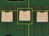
In looking at the picture and blowing it up, I note there are many unplated holes all around these parts. Are some underneath the parts? If so, air currents would be moving the parts. Also, this does not appear to be a bottom terminated component, as a large terminal is apparent on the lower end and two smaller terminals on the "legs" on the upper end of the component, so I don't think any of the comments regarding overprinting, etc, apply. If it does have a bottom termination, then they do. The vias along the top edge show wetting to the pads. Possibly getting the pads out from under the part may help.
Advanced Engineer/Scientist General Dynamics Richard D. Stadem is an advanced engineer/scientist for General Dynamics and is also a consulting engineer for other companies. He has 38 years of engineering experience having worked for Honeywell, ADC, Pemstar (now Benchmark), Analog Technologies, and General Dynamics.
|
|||||||
| Submit A Comment | |||||||
|
Comments are reviewed prior to posting. You must include your full name to have your comments posted. We will not post your email address. |
|
Free Newsletter Subscription
Circuitnet is built for professionals who bear the responsibility of looking ahead, imagining the future, and preparing for it. Insert Your Email Address |
|

|


